 Skip to main content
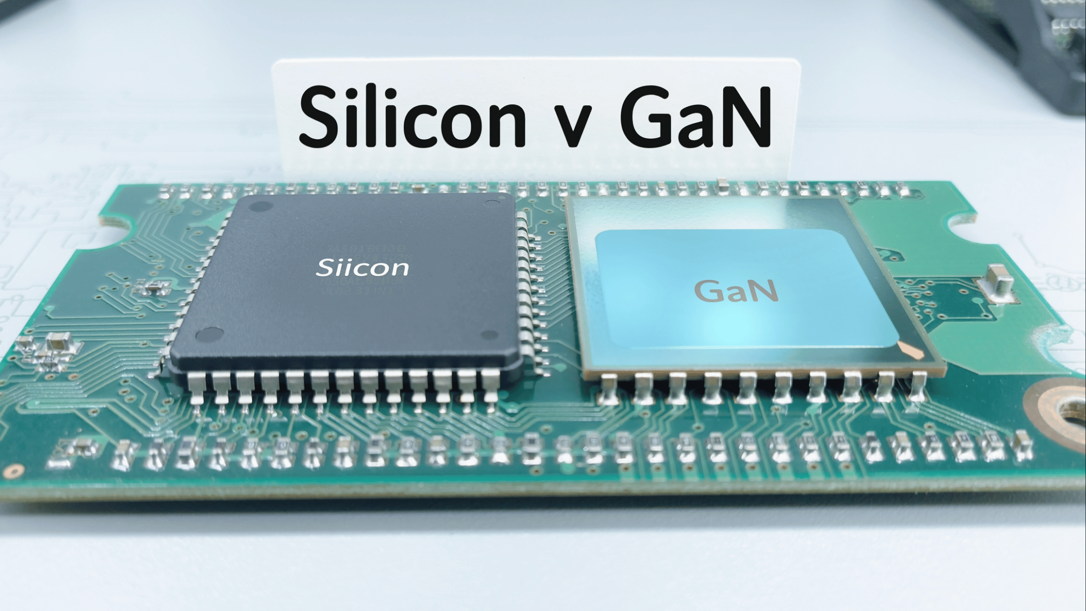
What Is GaN? And Why It’s Changing Power Supply Design
Gallium Nitride is reshaping how modern power supplies are specified and designed. As electronic products demand higher efficiency, smaller footprints, and tighter thermal control, traditional silicon solutions are starting to hit practical limits. Design teams need more flexibility at the power stage. This technology provides that flexibility without compromising performance.
The shift is driven by real engineering pressures. Power density targets are rising. Enclosure sizes are shrinking. Thermal margins are tighter. Wide bandgap devices help address all three when specified correctly.
What This Technology Means in Power Electronics
Gallium Nitride is a wide bandgap semiconductor material first developed for high-frequency and high-power applications. In power conversion, it supports much faster switching than silicon while reducing energy losses during operation. That combination makes it well suited to modern AC/DC and DC/DC designs.
Silicon remains a reliable and widely used option. This newer material builds on that foundation by removing many of the physical constraints engineers now face when designing compact, efficient power systems.
How It Differs from Silicon
The performance gap comes down to how each material handles voltage, heat, and switching behaviour. These devices switch at significantly higher frequencies and generate less heat during operation. This allows designers to reduce the size of transformers and passive components, which directly impacts overall PSU size and weight.
That capability explains why this approach is increasingly used in compact external adapters and desktop power supplies where mechanical space and thermal headroom are limited.
Efficiency Gains That Matter in Real Designs
Power supplies based on wide bandgap devices typically deliver higher efficiency across a wider load range compared to equivalent silicon designs. Lower losses translate into lower operating temperatures, which helps with compliance and overall system stability. In many external power supply designs, higher efficiency can support compliance with energy efficiency requirements such as Level VI, depending on the product and application.
Efficiency improvements also reduce stress on surrounding components, which supports long-term reliability.
Smaller Designs Without Compromise
Higher switching frequencies allow power stages to shrink without sacrificing electrical performance. Designers gain more usable power in less space, cleaner mechanical layouts, and greater freedom when packaging the final product.
This is especially valuable in ITE, AV, computing, and control systems where enclosure size often dictates early design decisions and limits later changes.
Thermal Performance and Long-Term Stability
Lower switching losses reduce heat generation at the source. That reduces dependence on bulky heatsinks and simplifies thermal design across the system. For OEMs, this lowers thermal risk during design-in and improves stability in demanding operating environments.
Better thermal control also supports longer service life and more consistent output performance over time.
Material-Level Validation Beyond Power Electronics
The performance advantages discussed here are not limited to power conversion alone. Research across other GaN-based technologies, including optoelectronic and photonic systems, consistently highlights the same underlying material strengths. These include wide bandgap behaviour, strong thermal stability, and reliable operation in demanding environments.
While the end applications differ, the material properties remain the same. That consistency helps explain why GaN performs well in compact, high-performance power designs where temperature, efficiency, and long-term stability are tightly linked.
Cleaner Output for Sensitive Electronics
Faster switching combined with improved control enables tightly regulated outputs with low ripple and noise. Audio, video, and data-driven systems depend on this stability to protect sensitive circuitry and maintain performance. This technology supports those requirements without forcing oversized power stages.
Practical Design Considerations
While the benefits are clear, there are design considerations that need attention early. Higher switching frequencies place greater importance on PCB layout, grounding, and EMI control. Poor layout choices can quickly erode performance gains.
A recent review of wide bandgap DC-DC converters for EV fast charging highlights EMI mitigation, thermal management, advanced gate driving, and high-frequency magnetics as key design areas. It also flags reliability topics such as dynamic RDS(on), gate degradation, and packaging stress. The same themes apply whenever you push power density and switching speed in compact designs.
EV Fast Charging Use Case

EV fast charging puts power conversion under extreme pressure. High power levels. Tight thermal budgets. Demanding EMC environments. That’s exactly why the EV market has become a proving ground for wide bandgap conversion stages.
The same ScienceDirect review reports converter examples achieving greater than 97% efficiency across a 100 W to 40 kW range and positions the 400–900 V class as a key segment for adoption in charger infrastructure.
A published on-board charger example shows what this approach enables in practice. A 6.6 kW bidirectional design using 650 V devices reports up to 96% efficiency and a power density of 2.2 kW/L, combining a totem-pole PFC stage with a dual active bridge DC-DC stage. This demonstrates what’s achievable when switching speed, magnetics, thermal design, and control are handled correctly.
Where This Approach Makes the Most Sense
The strongest return appears in applications where power density, efficiency, and thermal performance are critical. At higher power levels or in compact enclosures, the advantages are clear. In lower-power or cost-sensitive designs, silicon may still be the better choice.
Understanding where this technology adds real value helps avoid over-specification and keeps total system cost under control.
EMC and Compliance Considerations
Power supplies using wide bandgap devices can meet the same global safety and EMC standards as silicon designs, but system-level compliance still depends on correct integration. Early consideration of EMC behaviour, grounding strategy, and enclosure design reduces testing risk later in the project.
Specifying this type of solution early allows these factors to be addressed upfront rather than corrected after hardware is fixed.
Why This Matters at the Design Stage
For design engineers, the value lies in flexibility rather than a single performance gain. Smaller power stages, simpler thermal management, and easier efficiency compliance reduce redesign risk as projects move from prototype to production. Late-stage changes to the power supply often trigger mechanical and thermal knock-on effects that are difficult to resolve.
Designing with this approach from the outset avoids those issues.
Power Supply Support from Ideal Power
At Ideal Power, our GaN power supply ranges support both development and production environments. You get wide input voltage ranges, regulated outputs across multiple voltage options, and global safety approvals including UL, CE, UKCA, and IEC 62368-1. Performance stays consistent from prototype through volume supply.
Our team supports specification, selection, and long-term supply, helping you choose the right solution based on your application, environment, and compliance requirements.