 Skip to main content
7 Costly Power Supply Mistakes Engineers Keep Making
Power supplies are the core of all electronic systems; however, designing their layouts remains one of the most challenging tasks in engineering. Mistakes in power supply layouts cause voltage instability, increased electromagnetic interference (EMI), overheating, and premature component failure. These issues are especially problematic in electronic devices. These issues lead to costly product recalls, dissatisfaction, and expensive redesign cycles.
Despite advances in technology and design tools, many engineers continue to repeat avoidable errors when specifying and laying out power supply units (PSUs). Understanding these mistakes and how to avoid them is essential for delivering reliable, efficient, and compliant products. It is also important to have a solid understanding of electricity and electrical safety, as improper handling or design can lead to dangerous situations or damage.
This guide breaks down seven of the most common layout mistakes engineers make, providing detailed explanations, examples, and best practices to ensure your power supply designs withstand the demands of modern electronics.

Why layout quality defines reliability
Delivering stable, efficient power to a circuit depends on more than just a good specification. Engineers must determine the correct placement and configuration of connectors, power cables, PCB traces, and components, as well as understand the functions of these elements in ensuring consistent power delivery.
One misstep, such as a fragmented ground plane, can lead to noise, overheating, or unexpected resets. In sectors demanding high performance and reliability, layout errors remain a major contributor to field failures. Ensuring correct power delivery to critical components is essential for system stability.
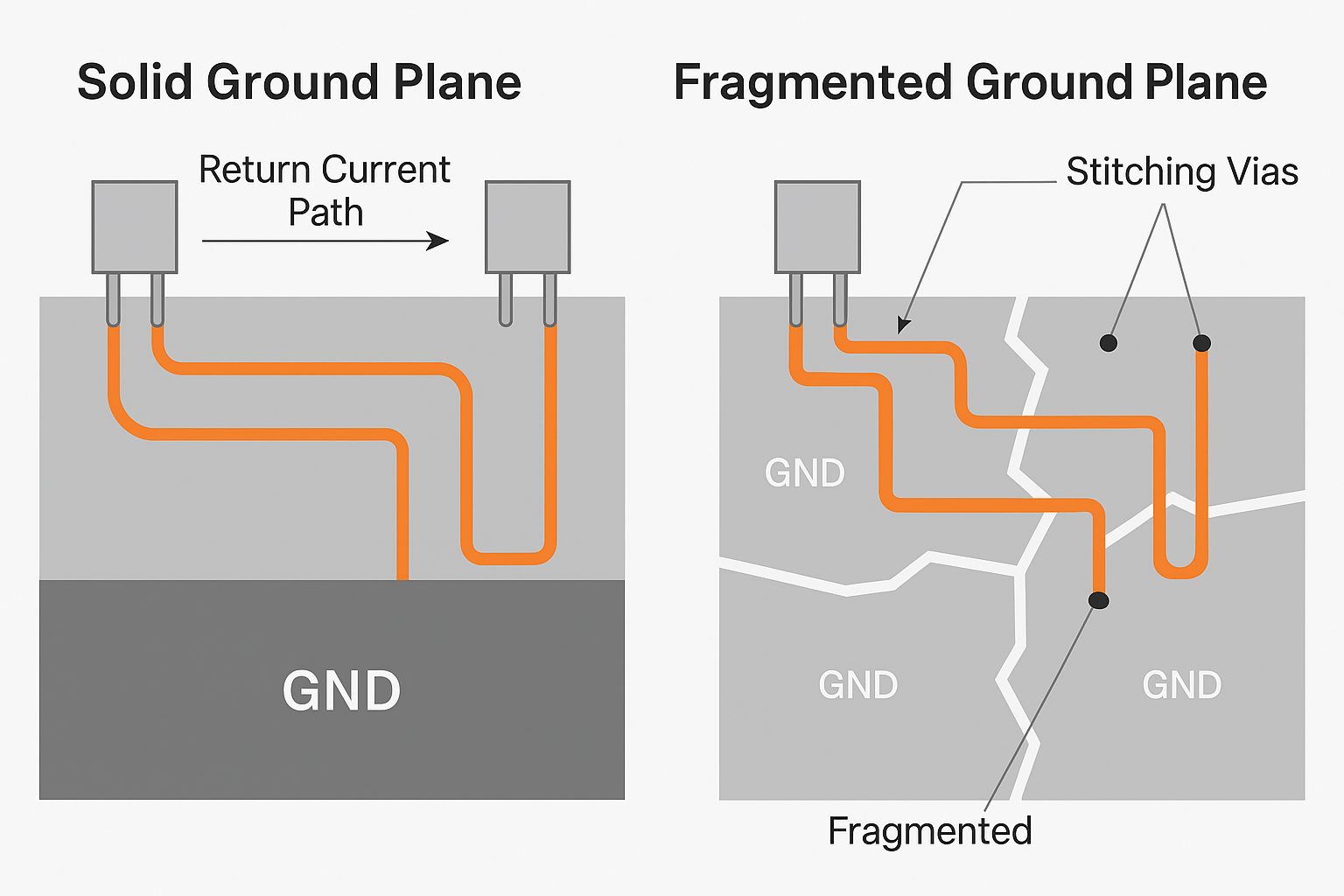
Poor Ground Plane Design
A continuous, well-planned ground plane is fundamental. It is the primary return path for current, and, in addition, a well-designed ground plane also supports stable operation of each power rail by minimising voltage fluctuations between rails. It provides essential shielding against electromagnetic interference (EMI). In power electronics, especially with switching components, maintaining a solid ground plane is critical to reducing noise coupling and preserving signal integrity.
Common errors include segmenting ground domains without a carefully planned low-impedance junction. This fragmentation forces return currents along less efficient paths, causing voltage fluctuations that impair system stability. These issues often occur when analogue and digital grounds are separated improperly without star grounding or stitching vias.
Best practice involves keeping a continuous ground plane beneath switching nodes, bridging splits with stitching vias, connecting analogue and digital grounds at a single low-current point, and extending ground planes beyond active circuitry to enhance shielding.
Undersized PCB Traces and Power Cables
Using traces or connectors that cannot handle the intended current leads to voltage drops, excessive heating, and eventual damage. Narrow traces increase resistance, causing localised heat build-up which degrades materials and threatens reliability. This happens when trace widths are reduced to save board space without recalculating current capacity or when repurposing connectors designed for lower currents. Overloading connector pins can cause overheating and mechanical failure.
Ignoring this can lead to voltage sag under load, degraded performance, intermittent faults, or total failure. Best practice includes sizing traces using IPC standards (for example, 1oz copper carrying 5A requires roughly 1.3mm trace width), distributing current across multiple pins or rails, using thicker copper or parallel traces, and confirming connector ratings.
Always check the maximum and max current ratings for each connector type to avoid exceeding safe limits and ensure reliable operation. Selecting a PSU that supplies sufficient power for the entire system also prevents underpowering issues.
Incorrect Component Placement
Placing heat-generating components too close or near sensitive parts restricts airflow, and improper fan placement can further exacerbate thermal issues and cause thermal hotspots. This raises junction temperatures, accelerating component ageing and reducing efficiency. Temperature-sensitive devices such as electrolytic capacitors are especially vulnerable.
Thermal simulations and airflow modelling help identify these hotspots before finalising layouts. Best practice is to space high-heat components and inductors to allow direct airflow and position sensitive parts away from heat sources. Additionally, ensure that airflow strategies and proper fan orientation help keep components cool.
Missing or Poor Thermal Vias
Insufficient thermal vias under hot components hinder heat dissipation, causing elevated temperatures and reducing lifespan.
This often results from inadequate via density, plating, or spacing, sometimes overlooked due to lack of thorough thermal analysis. Thermal simulations and imaging reveal poor via placement.
Proper design uses dense arrays of small, plated vias beneath thermal pads, connected to internal copper planes, significantly lowering junction temperatures and improving reliability.
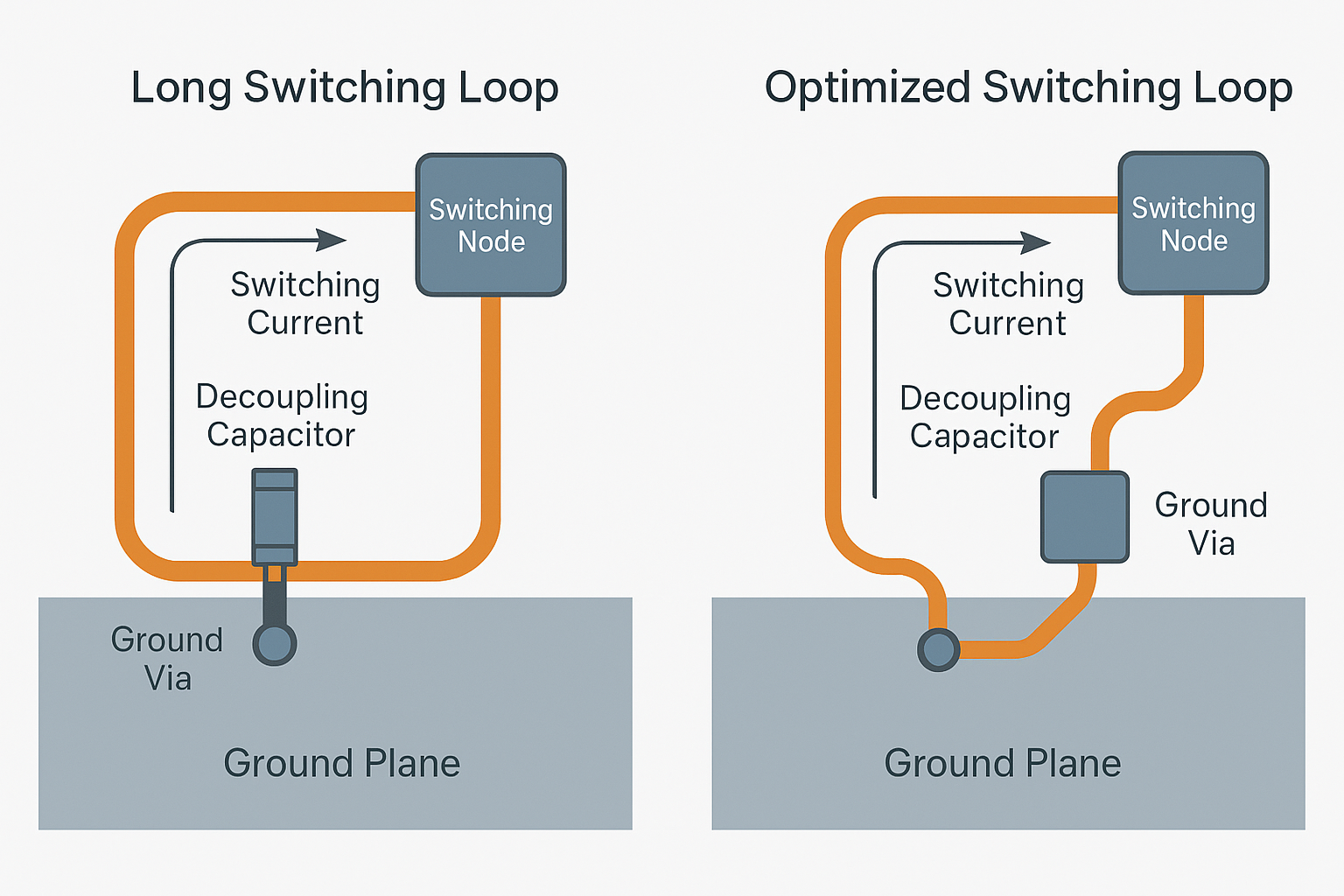
Excessive Loop Inductance from Poor Trace Routing
Long or narrow switching loops increase parasitic inductance, causing voltage overshoot, ringing, and EMI. These effects raise ripple and noise, harming regulation and EMC performance.
Inductance simulations and EMI scans help detect such problems. To reduce inductance, keep switching components close, route wide and direct traces, position decoupling capacitors within 1 to 2 mm of power pins, maintain continuous ground planes, and use orthogonal routing layers to isolate noisy signals.
Ground Loop Formation
Ground loops arise from multiple return paths forming closed loops that pick up electromagnetic noise. They commonly occur in mixed-signal systems with improper grounding or cable routing.
Ground loops increase noise, degrade signal stability, and often fail EMC testing. Prevent them by using star grounding where all grounds meet at a single low-impedance node, separating analogue and digital grounds until that point, and ensuring proper shielding and defined ground returns in multi-board systems.
Flawed Power Delivery Network (PDN) Design
The PDN must maintain stable voltage and current despite load changes. Poor PDN layouts cause voltage drops, ripple, slow transient response, and instability.
Impedance simulations across frequency and load ranges detect resonances and weak points. Inadequate PDN design lowers the power supply rejection ratio, allowing input noise to affect circuits.
Best practices include placing bulk and decoupling capacitors close to load pins, minimising dielectric thickness between power and ground planes, using thick copper layers, multiple vias, and validating PDN performance through simulation. Additionally, collecting and analysing power consumption data, such as historical wattage output and power usage trends, can further optimise the PDN.
Prevention and Best Practices
Begin with a clear understanding of continuous and peak load demands for your system. Accurately estimating these loads is crucial to selecting the right power supply unit (PSU) that can handle both everyday operation and occasional surges without failure. Use detailed simulations to analyse electrical, thermal, and electromagnetic interference (EMI) performance under varying conditions and parameters.
Build and rigorously test prototypes under realistic load scenarios to verify thermal stability, EMI compliance, and voltage regulation. During testing, carefully protect sensitive components and monitor key metrics to identify potential issues early.
Leverage a variety of online simulation tools and technical resources to refine your designs before moving to production. This proactive approach helps avoid costly field failures, ensures adherence to certification standards, and ultimately leads to more reliable and robust power supply layouts.
Why Choose Ideal Power?
Ideal Power brings decades of expertise in supplying and supporting high-quality internal power supply PSUs tailored to demanding industrial and commercial applications. Our commitment to engineering excellence ensures customers receive components and services that meet stringent performance and regulatory requirements.
From early-stage design consultations to post-installation support, our team helps engineers specify their PSU early, optimise layouts, and navigate complex challenges such as thermal management and EMI compliance.
Want to avoid these layout errors in your next design? Book a 15-minute PSU layout review with one our engineers.